Tutorials using KOH
(Summary description)
- Categories:Software case
- Author:
- Origin:
- Time of issue:2022-06-28
- Views:473
Tutorial I-1: Convex corners
Source:Schröder et al., JMM 10 (2000) 88-97.
1. efine siliconsample:
Si(100) with <110> flat, 2500x2500μm2,NOC =256.
2. Apply nitridemask:
Choose mask “demo-I-1-1.bmp”. Apply asNITRIDE.
3. Wet etching:
Use “KOH 40 wt 81 C” for 140 μm (etch bydepth).
6. Remove thenitride mask:
Select “Material: nitride” and press on“Remove layer from top” button.

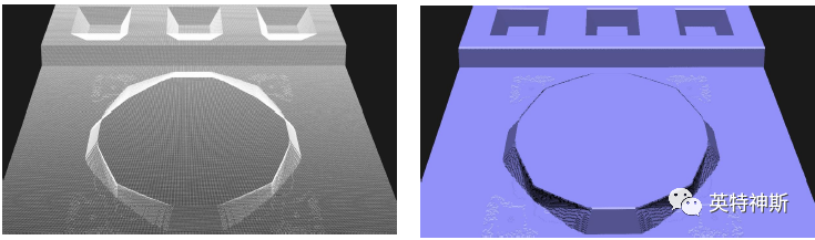
Figure 1: Comparison between experiment (top) and simulation (bottom) for Tutorial I-1. The etch depth is approx. 140 μm.
Tutorial I-2: AFM tip
Source: C. Liu, Foundations of MEMS, Pearson Prentice Hall, ISBN 0-13-147286-0,(Fig. 10-3-1)
1. Define silicon sample:
Si(100) with <100> flat, 250x250 μm2, NOC = 256.
Cut crystal at depth: 22 μm (“two layers” creates top and bottom surfaces).
2. Apply nitride mask to the top side:
Choose mask “demo-I-2-1.bmp”. Apply on top side as NITRIDE.
3. Apply nitride/oxide masks to the bottom side:
Choose mask “demo-I-2-2.bmp”. Apply on bottom side as NITRIDE.
Choose mask “demo-I-2-3-LOCOS.bmp”. Apply on bottom side as OXIDE.
4. Wet etching:
Use “KOH 40 wt 70 C” for 17 min (etch by time).
5. Remove the nitride mask form the top side:
Select “Material: nitride” and press on “Remove layer from top” button.
6. Apply nitride mask to the top side:
Choose mask “demo-I-2-4.bmp”. Apply on top side as NITRIDE.
7. Wet etching:
Use “KOH 40 wt 70 C” for 28 min (additional 11 min).
8. Remove the oxide mask from the bottom side:
Select “Material: oxide” and press on “Remove layer from bottom” button.
9. Wet etching:
Use “KOH 40 wt 70 C” for 35 min (additional 7 min).
10. Remove the nitride masks from the top and bottom:
Select “Material: nitride” and press on “Remove layer from top” button.
Select “Material: nitride” and press on “Remove layer from bottom” button.
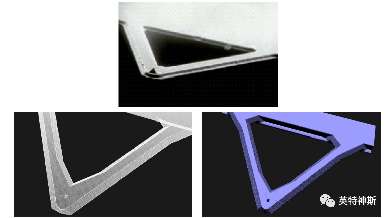
Figure 2: Comparison between experiment (top) and simulation (bottom) for Tutorial I-2.
Tutorial I-3: Cantilever array
Source: Daisuke et al., Sensors and Actuators A 95 (2002) 281-287.
1. Define silicon sample:
Si(100) with <100> flat, 200x200 μm2, NOC = 256.
Define as SOI wafer with: Depth = 5 μm, Thickness = 5 μm.
2. Apply nitride mask to the top side:
Choose mask “demo-I-3-1.bmp”. Apply on top side as NITRIDE.
3. 1st wet etching:
Use “KOH 30 wt 70 C” for 4 μm (etch by depth, approx. 6.5 min).
4. Protect with oxide the exposed silicon:
Choose mask “demo-I-3-2-LOCOS.bmp”. Apply on top side as OXIDE.
5. Remove the nitride mask form the top side:
Select “Material: nitride” and press on “Remove layer from top” button.
6. Apply nitride mask to the top side:
Choose mask “demo-I-3-3.bmp”. Apply on top side as NITRIDE.
7. 2nd wet etching:
Use “KOH 30 wt 70 C” until 23 min (additional 16.5 min).
8. Protect with oxide the exposed silicon:
Choose mask “demo-I-3-4-LOCOS.bmp”. Apply on top side as OXIDE.
9. Remove the nitride mask form the top side:
Select “Material: nitride” and press on “Remove layer from top” button.
10. 3rd wet etching:
Use “KOH 30 wt 70 C” until 45 min (additional 22 min).
11. Remove the oxide mask form the top side:
Select “Material: oxide” and press on “Remove layer from top” button.

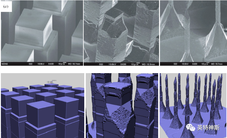
Figure 3: Comparison between experiment/theory (top) and simulation (bottom) for Tutorial I-3.
Tutorial I-4: Microneedles
Source: Shikida et al., J. Micromech. Microeng. 14 (2004) 1462-1467.
1. Define silicon sample:
Si(100) with <110> flat, 600x600 μm2, NOC = 184.
2. Apply oxide mask to the top side:
Choose mask “demo-I-4-1.bmp”. Apply on top side as OXIDE.
3. Vertical etching:
DRIE etch for 240 μm.
4. Remove the oxide mask from the top side:
Select “Material: oxide” and press on “Remove layer from top” button.
5. Apply oxide mask to the top side:
Choose mask “demo-I-4-2.bmp”. Apply on top side as OXIDE.
6. Vertical etching:
DRIE etch for 320 μm (additional 80 μm).
7. Remove the oxide mask from the top side:
Select “Material: oxide” and press on “Remove layer from top” button.
8. Wet etching:
Use “KOH 40 wt 70 C” for 38 min (etch by time).
Figure 4: Comparison between experiment (top) and simulation (bottom) for Tutorial I-4. Left: after second vertical etch. Center: after wet etching for 20 min. Right: after wet etching for 38 min.
Tutorial I-5: 3-axis accelerometer
Source: Schröpfer et al., J. Micromech. Microeng. 8 (1998) 77–79.
1. Define silicon sample:
Si(100) with <100> flat, 3780x2520 μm2, NOC = 384.
Cut crystal at depth: 70 μm (“two layers” creates top and bottom surfaces).
2. Apply nitride mask to the top side:
Choose mask “demo-I-5-1.bmp”. Apply on top side as NITRIDE.
3. Apply nitride mask to the bottom side:
Use same mask “demo-I-5-1.bmp”. Apply on bottom as NITRIDE.
4. Wet etching:
Use “KOH 40 wt 70 C” for 20 min (etch by time).
5. Remove pattern from top and bottom nitride masks:
Choose mask “demo-I-5-2.bmp”.
Select “Material: nitride” and press on “Remove pattern from top” button.
Select “Material: nitride” and press on “Remove pattern from bottom” button.
6. Wet etching:
Use “KOH 40 wt 70 C” for 65 min (additional 45 min).
7. Remove the nitride mask from the top and bottom sides:
Select “Material: nitride” and press on “Remove layer from top” button.
Select “Material: nitride” and press on “Remove layer from bottom” button.
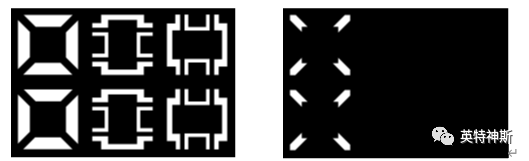
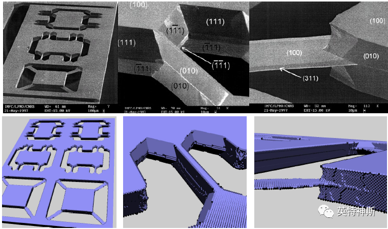
Figure 5: Comparison between experiment (top) and simulation (bottom) for Tutorial I-5.
Tutorial I-6: Perfect convex corners
Source: Pal et al., J. Micromech. Microeng. 14 (2004) 1416-1420.
1. Define silicon sample:
Si(100) with <110> flat, 200x200 μm2, NOC = 256.
Define as SOI wafer with: Depth = 12 μm, Thickness = 10 μm.
2. Apply oxide mask to the top side:
Choose mask “demo-I-6-1.bmp”. Apply on top side as OXIDE.
3. Apply nitride mask to the top side:
Choose mask “demo-I-6-2.bmp”. Apply on top side as NITRIDE.
4. Remove pattern from top oxide mask:
Choose mask “demo-I-6-2.bmp” (same as in previous step).
Select “Material: oxide” and press on “Remove layer from top” button.
4. Wet etching:
Use “KOH 40 wt 70 C” for 30 min (etch by time).
5. Passivate the etched regions using LOCOS process (oxide is “grown”):
Choose mask “demo-I-6-3-LOCOS.bmp”. Apply on top side as OXIDE.
6. Remove the nitride mask from the top side:
Select “Material: nitride” and press on “Remove layer from top” button.
7. Wet etching:
Use “KOH 40 wt 70 C” for 70 min (additional 40 min).
8. Remove the oxide mask from the top side:
Select “Material: nitride” and press on “Remove layer from top” button.
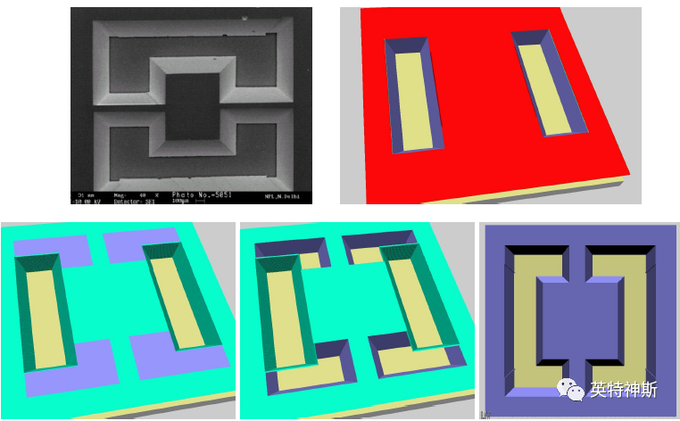
Figure 6: Comparison between experiment (top-left) and simulation (top-right and bottom) for Tutorial I-6. Bottom left, center and right correspond to the state after step 6, 7 and 8, respectively.
Tutorial I-7: Microfluidic channels
Source: J. W. Kwon et al., Sensor and Actuators A 97-98 (2002) 729-733.
1. Define silicon sample:
Si(100) with <110> flat, 1000x1000 μm2, NOC = 256.
2. Apply nitride mask to the top side:
Choose mask “demo-I-7-1.bmp”. Apply on top side as NITRIDE.
3. Wet etching:
Use “KOH 40 wt 70 C” for 60 min (etch by time).
4. Remove the nitride mask from the top side:
Select “Material: nitride” and press on “Remove layer from top” button.
5. Apply nitride mask to the top side:
Choose mask “demo-I-7-2.bmp”. Apply on top side as NITRIDE.
6. Wet etching:
Use “KOH 40 wt 70 C” for 120 min (additional 60 min).
7. Remove the nitride mask from the top side:
Select “Material: nitride” and press on “Remove layer from top” button.
8. “Grow” polysilicon on selected regions of the top side:
Choose mask “demo-I-7-3.bmp”. Apply on top side as POLYSILICON.
9. Apply nitride mask to the top side:
Choose mask “demo-I-7-4.bmp”. Apply on top side as NITRIDE.
10. Wet etching:
Use “KOH 40 wt 70 C” for 180 min (additional 60 min).
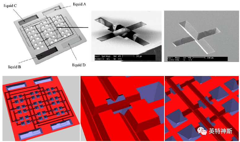
Figure 7: Comparison between experiment (top) and simulation (bottom) for Tutorial I-7.
Tutorial I-8: Micromachining on (111)
Source: S. Park et al., Jpn. J. Appl. Phys. 38 (1999) 4244-4249.
1. Define silicon sample:
Si(111) with <110> flat, 100x100 μm2, NOC = 256.
2. Apply oxide mask to the top side:
Choose mask “demo-I-8-1.bmp”. Apply on top side as OXIDE.
3. Vertical etching:
DRIE etch until a depth of 2 μm.
4. Passivate the etched regions using LOCOS process (oxide is “grown”):
Choose mask “demo-I-8-2.bmp”. Apply on top side as OXIDE.
5. Remove pattern from top oxide mask:
Choose mask “demo-I-8-1.bmp” (the same as in step 1).
Select “Material: oxide” and press on “Remove pattern from top” button.
6. Vertical etching:
DRIE etch until 4 μm (additional 2 μm).
7. Wet etching:
Use “KOH 40 wt 70 C” for 30 min (etch by time).
8. Remove the oxide mask from the top side:
Select “Material: oxide” and press on “Remove layer from top” button.
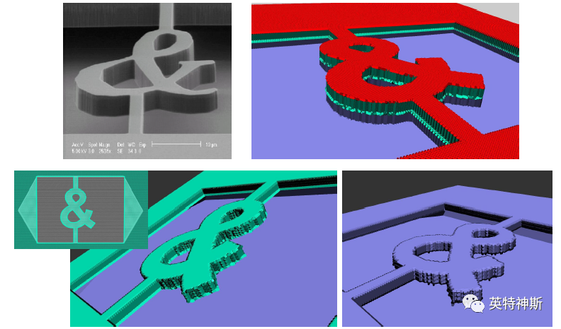
Figure 8: Comparison between experiment (top-left) and simulation (top-right and bottom) for Tutorial I-8. Top-right: state after step 5 showing the first and second oxides in red and light green, respectively. Bottom left and center: top view and 3D view after step 7, respectively. Bottom-right: state after step 8.
Tutorial I-9: {111} plates in Si{100}
Source: J. W. Berenschot et al., J. Micromech. Microeng. 8 (1998) 104-106.
1. Define silicon sample:
Si(100) with <110> flat, 100x100 μm2, NOC = 256.
Cut crystal at depth: 10 μm (“two layers” creates top and bottom surfaces).
2. Apply nitride mask to the top side:
Choose mask “demo-I-9-1.bmp”. Apply on top side as NITRIDE.
3. Apply nitride mask to the bottom side:
Choose mask “demo-I-9-2.bmp”. Apply on bottom side as NITRIDE.
4. Wet etching:
Use “KOH 40 wt 70 C” for 20 min (etch by time).
5. Remove the nitride mask from the top and bottom sides:
Select “Material: nitride” and press on “Remove layer from top” button.
Select “Material: nitride” and press on “Remove layer from bottom” button.
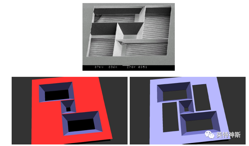
Figure 9: Comparison between experiment (top) and simulation (bottom) for Tutorial I-9. Bottom-left: after step 5. Bottom-right: after step 5.
Tutorial I-10: Prismatic beams
Source: H. Hu et al., Sensors and Actuators A 93 (2001) 258-265.
1. Define silicon sample:
Si(100) with <110> flat, 100x100 μm2, NOC = 256.
2. Apply oxide mask to the top side:
Choose mask “demo-I-10-1.bmp”. Apply on top side as OXIDE.
3. Vertical etching:
DRIE etch until a depth of 30 μm.
4. Wet etching:
Use “KOH 40 wt 70 C” for 6 min (etch by time).

Figure 10: Comparison between theory (top) and simulation for Tutorial I-10: Middle-left: after step 3. Middle-right and bottom-left: after wet etching for 3 min. Bottom-center and bottom-right: after wet etching for 6 min.
Tutorial I-11: Etching spheres
Source: K. Sato et al., Sensors and Actuators A 61 (1998) 87-93.
1. Define silicon sample:
“Simulation” → “Create <011> sphere”
2. Save the initial state of the sphere:
“File” → “Export sphere coordinates...”
Give a name, such as “demo-I-11_SphereCoordinates_BeforeEtching.txt”.
3. Wet etching:
Choose the etchant and etch by time.
Example: KOH 40 wt 70 C, 480 min.
4. Save the final state of the sphere after etching:
“File” → “Export sphere coordinates...”
Give a name, such as “demo-I-11_SphereCoordinates_KOH40wt70C_480min.txt”.
5. Visualize the etch rates:
a. Exit “GPUetch”.
b. Start “Experimental data viewer/Calibrator”.
c. “File” → “Load sphere data from simulator...”
d. Browse for the initial and final states of the sphere that were saved in steps 2 and 4:
Initial: “demo-I-11_SphereCoordinates_BeforeEtching.txt”
Final: “demo-I-11_SphereCoordinates_KOH40wt70C_480min.txt”.
Input the etching time, 480 min in this example.
e. Compare to experiment by selecting the corresponding etchant on the left panel.
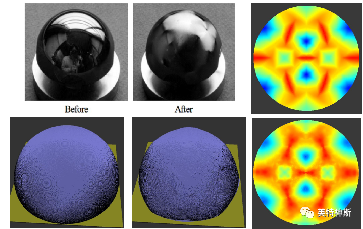
Figure 11-1: Comparison between experiment (top) and simulation (bottom) for Tutorial I-11.
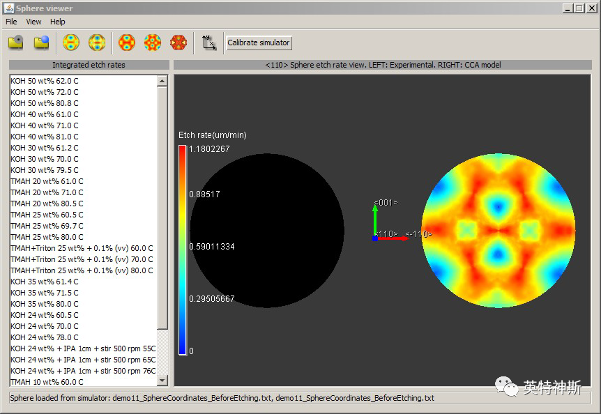
Figure 11-2: Experimental data viewer/Calibrator after step 5d of Tutorial I-11.
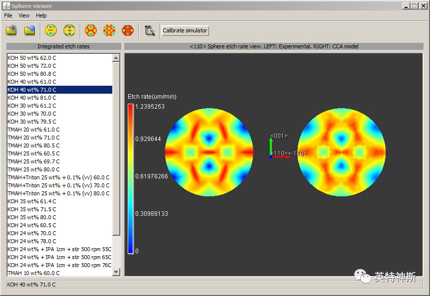
Figure 11-3: Experimental data viewer/Calibrator after step 5e of Tutorial I-11. The visualized scene
can be rotated, relocated and zoomed in/out.
Tutorial I-12: Dual-axis micromechanical probe
Source: Fukuzawa et al., J. Appl. Phys. 101 (2007) 034308.
1. Define silicon sample:
Si(100) with <100> flat, 4000x4000 μm2, NOC = 256.
Cut crystal at depth: 190 μm (“two layers” creates top and bottom surfaces).
2. Apply nitride mask to the top side:
Choose mask “demo-I-12-1.bmp”. Apply on top side as NITRIDE.
3. Apply nitride mask to the bottom side:
Choose mask “demo-I-12-2.bmp”. Apply on bottom side as NITRIDE.
4. Wet etching:
Use “KOH 40 wt 70 C” for 80 min (etch by time).
5. Remove the nitride mask from the top and bottom sides:
Select “Material: nitride” and press on “Remove layer from top” button.
Select “Material: nitride” and press on “Remove layer from bottom” button.
6. Apply nitride mask to the top side:
Choose mask “demo-I-12-3.bmp”. Apply on top side as NITRIDE.
7. Apply nitride mask to the bottom side:
Choose mask “demo-I-12-1.bmp”. Apply on bottom side as NITRIDE.
8. Wet etching:
Use “KOH 40 wt 70 C” for 350 min (additional 270 min).
9. Remove the nitride mask from the top and bottom sides:
Select “Material: nitride” and press on “Remove layer from top” button.
Select “Material: nitride” and press on “Remove layer from bottom” button.
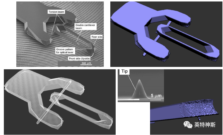
Figure 12: Comparison between experiment (top-left) and simulation for Tutorial I-12.
Tutorial I-13: Eight-beam proof mass
Source: Xiao et al., J. Micromech. Microeng. 18 (2008) 075005.
1. Define silicon sample:
Si(100) with <110> flat, 5040x5040 μm2, NOC = 256.
Cut crystal at depth: 700 μm (“two layers” creates top and bottom surfaces).
2. Apply oxide mask to the top and bottom sides:
Choose mask “demo-I-13-1.bmp”.
Apply on top side as OXIDE.
Apply on bottom side as OXIDE.
3. Wet etching:
Use “KOH 40 wt 70 C” for 60 min (etch by time).
4. Apply oxide mask to the top and bottom sides:
Choose mask “demo-I-13-2.bmp”.
Apply on top side as OXIDE.
Apply on bottom side as OXIDE.
5. Wet etching:
Use “KOH 40 wt 70 C” for 120 min (additional 60 min).
6. Remove the oxide mask from the top and bottom sides:
Select “Material: oxide” and press on “Remove layer from top” button.
Select “Material: oxide” and press on “Remove layer from bottom” button.
7. Apply oxide mask to the top side:
Choose mask “demo-I-13-3.bmp”. Apply on top side as oxide.
8. Apply oxide mask to the bottom side:
Choose mask “demo-I-13-4.bmp”. Apply on bottom side as oxide.
9. Vertical etching from the top and from the bottom:
DRIE etch until a depth of 150 μm (top side).
DRIE etch until a depth of 550 μm (bottom side).
10. Passivate the exposed silicon regions with a thermal oxide (LOCOS process):
Choose mask “demo-I-13-5.bmp”.
Apply on top side as OXIDE.
Apply on bottom side as OXIDE.
11. Remove pattern from top oxide layer:
Choose mask “demo-I-13-6.bmp”.
Select “Material: oxide” and press on “Remove pattern from top” button.
12. Remove pattern from bottom oxide layer:
Choose mask “demo-I-13-7.bmp”.
Select “Material: oxide” and press on “Remove pattern from bottom” button.
13. Wet etching:
Use “KOH 40 wt 70 C” for 780 min (additional 660 min).
14. Remove the oxide mask from the top and bottom sides:
Select “Material: oxide” and press on “Remove layer from top” button.
Select “Material: oxide” and press on “Remove layer from bottom” button.
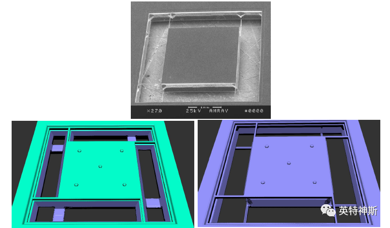
Figure 13(A): Comparison between experiment (top) and simulation for Tutorial I-13. Bottom-left:
After wet etching for 480 min during step 13. Bottom-right: After step 14.
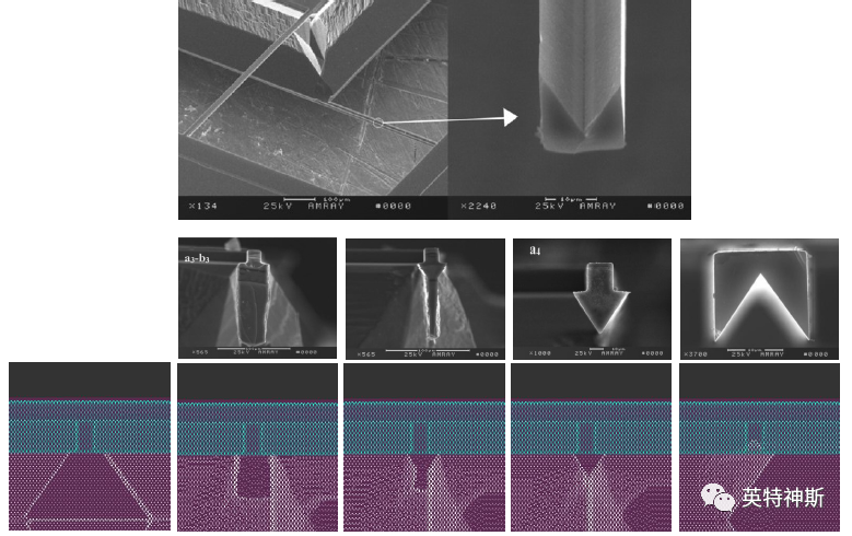
Figure 13(B): Comparison between experiment (top) and simulation for Tutorial I-13.
Scan the QR code to read on your phone
Applications
Learn how Intellisense can help you?
E-mail:china@intellisense.com
Add:No. 19, Lixin Road, Nanjing Jiangbei New Area, Nanjing City, Jiangsu Province


Copyright © 2022 Jiangsu Intellisense Technology Co.,Ltd. 苏ICP备08107867号 Powed by:300.cn SEO
 Tel
Tel Messages
 Top
Top